Message
Metamaterials laboratory have been pursuing studies on nano optics/photonics since the establishment of the laboratory on April 1 2008.
We are extensively exploring new optics and photon technologies exploiting various types of microscopes (especially three-dimensional microscopes), high power lasers, ultra-short-pulsed lasers, nano-fabrication technology, self-assembly phenomenon, living-cell manipulation, numerical analysis, and so on.
Recently we focus on artificial optical functional metallic nano structures, which is termed “metamaterials”, and three-dimensional multilayer terabyte optical storages.
Ultimate goal of optical technology is enabling manipulation of light (photon) propagation with our complete control. From a simple hand glass to a leading microscope and semiconductor fabrication devices, controlling behaviors of light is achieved solely by laying out appropriate refractive index distribution in a three-dimensional space with lenses, prisms, mirrors, and so on. Namely, a degree of freedom in manipulating light depends on varieties of distribution in refractive index (in other words, materials) and their arrangement in a space. Refractive index of material is defined as square root of its relative permittivity ε and relative magnetic permeability μ. According to traditional understanding in opticas, the value of μ is fixed to unity, and only the value of ε can be arranged by changing a choice of material. Thus, the lack of controllability of the value μ pretty much narrows range of freedom in designing refractive index of a material, inhibit us from freely controlling behaviors of light.
A material which can bring a breakthrough the present situation is a metamaterial, which is an artificial material consisting of arrays of noble metal nano structures. Those metallic nano structures are equivalent of atoms and/or molecules making up a material. Thus, ε and μ of a material can be tuned by arranging design and/or material of unit nanometer-scale structure regardless of material’s conventionally-defined ε and μ. This new approach overturns the long-held understanding that a material and it’s optical properties automatically correspondent each other, and opens new possibilities of science and technology in optics and optical materials.
In a text book of optics, many theoretical limits such as resolution limit are shown. However, those mathematical consequences were derived with respect to the prerequisite that the value of μ of natural substances equals to 1. If a world where the value of μ is other than unity would come true, limitations today would not be limitations any more. Actually, metamaterial-based optical devices have already proved to exibit extraordinary optical phenomena. Our group is challenging to realize the dream -ultimate control of light- using our metamaerial technologies.
Takuo TANAKA
April, 2009
Topics
Magnetic Assembly of Three-Dimensional Metamaterials
Fabrication of Plasmonic Split Ring Resonators via Self-Assembly
Plasmonic Nanostructures Fabricated by Nanocoating Lithography
Optical Properties of Gold Periodical Nanostructures
Surface Plasmon Triggering Metal-Insulator Transition
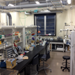
Facilities
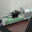
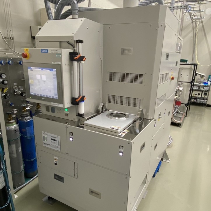
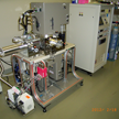
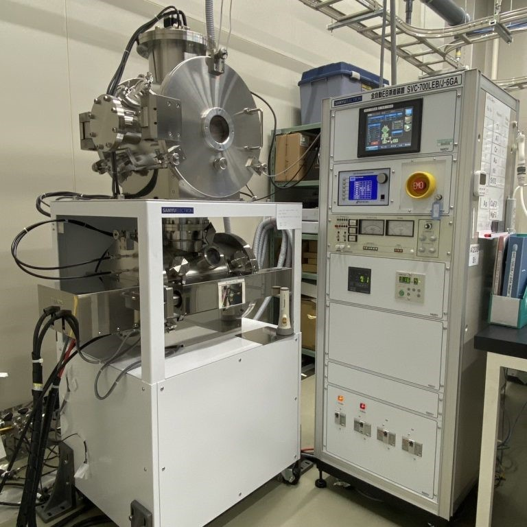
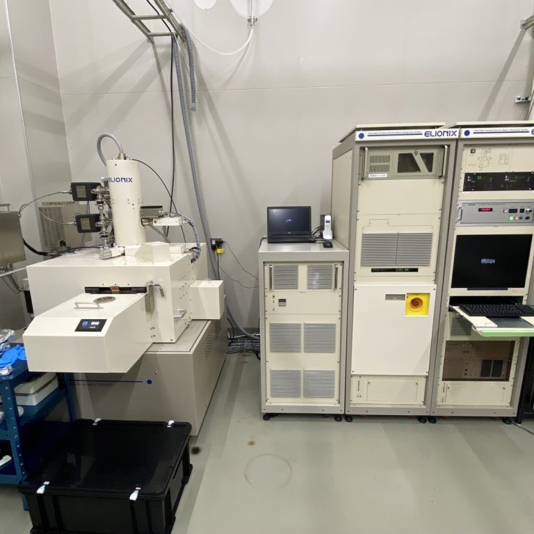
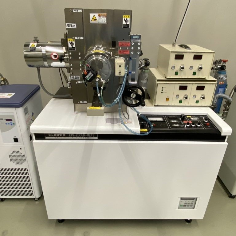
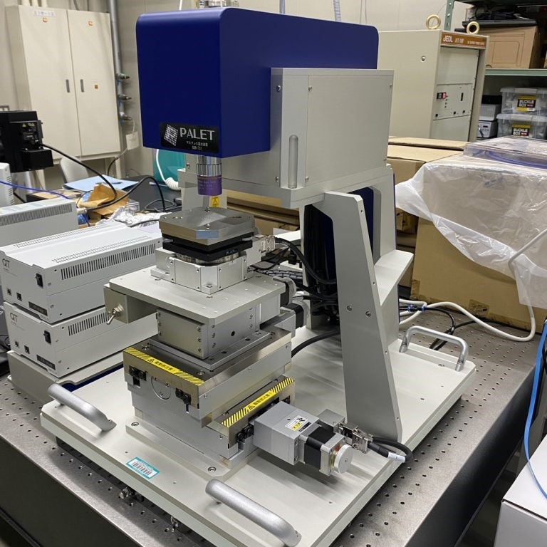
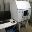
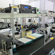
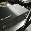
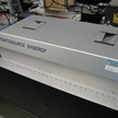
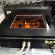
Fabrication Systems


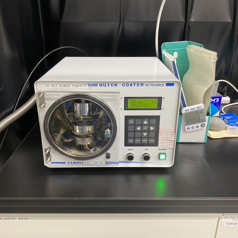
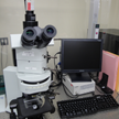
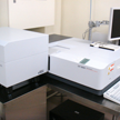
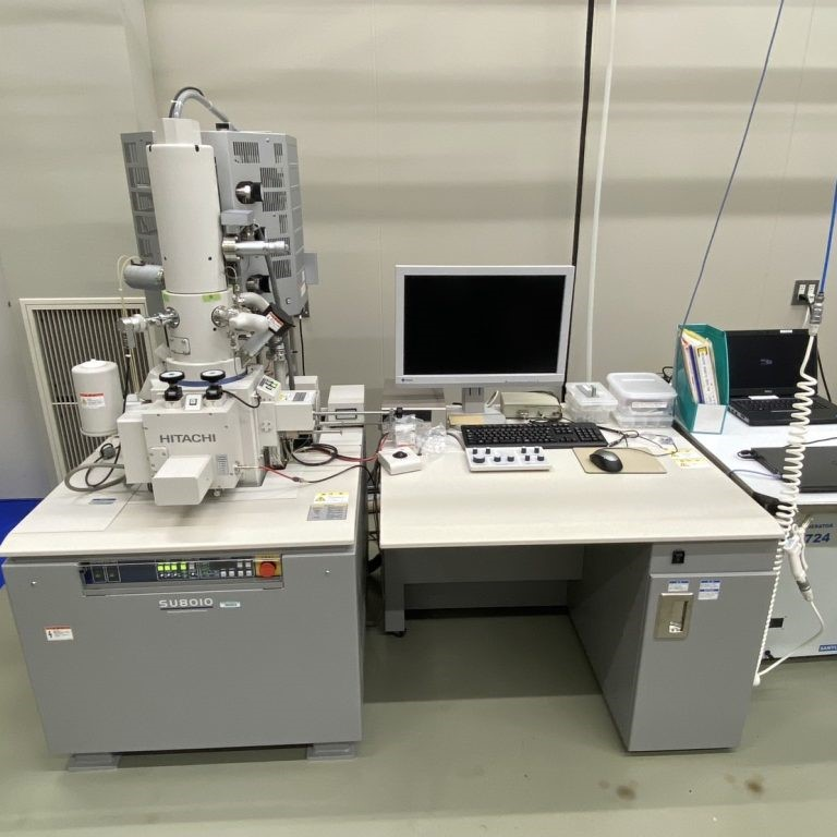
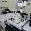
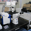
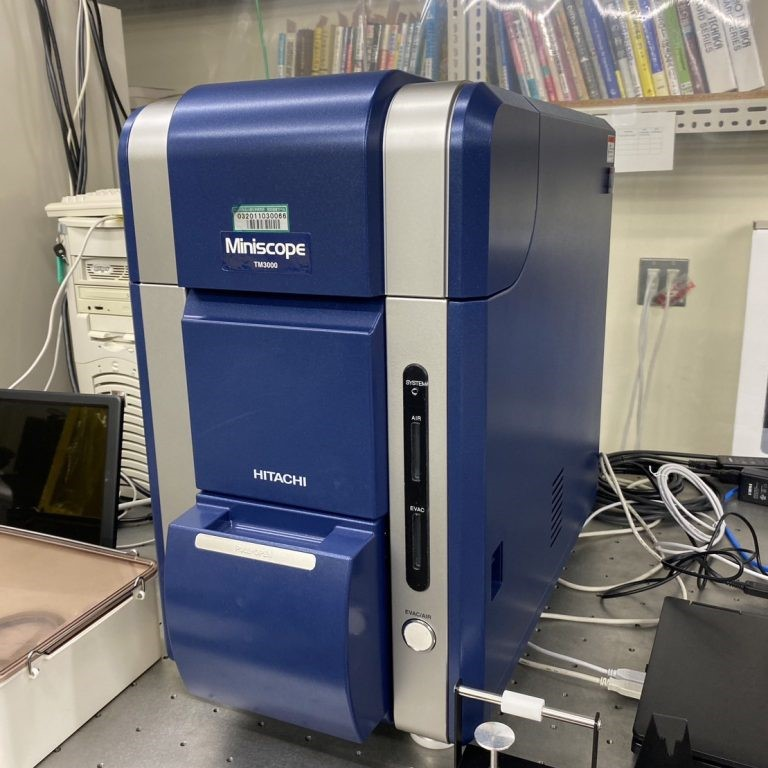
Characterization Systems

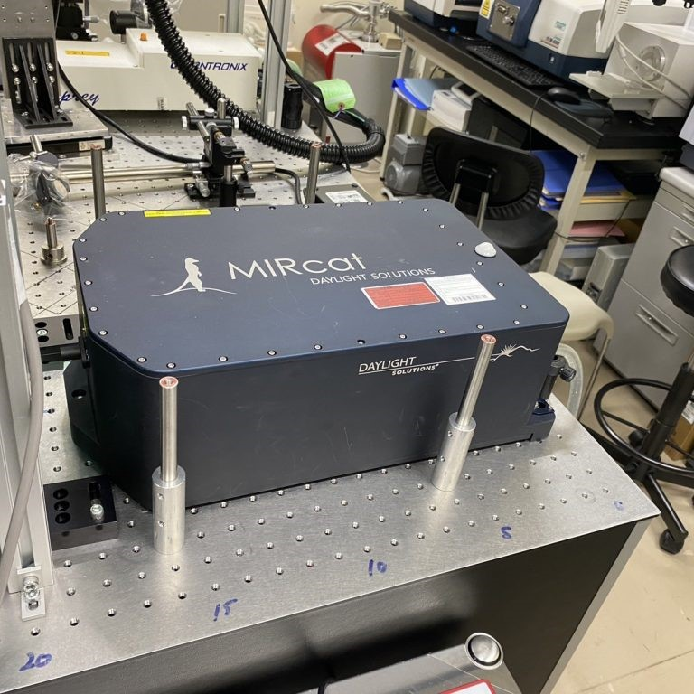
Laser systems

Numerical Simulations


Symposium
In this symposium, we have invited talks related to plasmonics and metamaterials. Research progresses of our group are also presented. For close communications with invited speakers, a small seminar room is selected as a venue.
RIKEN Metamaterials Symposium 2012
keywords: plasmonic biosensors, THz chemical and biological sensing
RIKEN Metamaterials Symposium 2011
keywords: quantum coupling, green device, gold nanorod
RIKEN Metamaterials Symposium 2010
(9th Metamaterials & Nanophotonics Symposium)
Contact: metssympo2012(at)mets.riken.jp 【Change (at) to @】
About the lab’s logo


The eyeglasses-like shape stands for two “m” s in a word “Metamaterial” as well as nano resonators; building blocks of metamaterials. The blue color attributed from the logo of Kawata nanophotonics laboratory, RIKEN (originally the color attributed from the RIKEN‘s logo). Then, red was selected as a new color since combination of red and blue is often used to represent plus and minus of electronics and N and S poles of magnetics; both of them are fundamental elements in electromagnetics. Gold and silver in frames literally represent gold and silver metals, which are key materials in plasmonics and plasmonic metamaterials.
How to join us
We welcome researchers from wide varieties of fields who are interested in developing optical technologies in nano-meter range. We greatly welcome pepole who are skilled in more than two categories in the followings. Skills in communication, discussion and writting in English are prerequisite.
1. Numerical simulation using FDTD, RCWA, and so on.
2. Establishment of optical system with femto second lasers, OPO, OPA, amplifiers, and so on.
3. Nano structure fabricaiton using self-assembly mechanism.
4. Nano fabrication technology using EB lithography, nano inprinting, vacuum evaporators, sputtering, and so on.
5. Observation and measurement using SEM, TEM, AFM, and STM.
6. Chemical approach to prepare metallic nano particles and rods.
7. Optical measurement in the range of far infrared wavelengths (THz).
Type of employment
We can accept new lab members with the following employment system.
1. Special Postdoctoral Researcher at RIKEN
2. Foreign Special Postdoctoral Researcher at RIKEN
3. JSPS Postdoctoral Researcher (There are various types of programs.)
This year’s recruitments are already closed. Please consider to apply above grants in the next year. Please contact us before you apply for these fellowship grants.